Looking to the Future of Carbon Nanotube Transistors
New review article from Professor Mark Hersam considers what’s next for the emerging technology
Integrated circuits (ICs) serve as the basis of computers, tablets, smartphones, and other technology that enhances our daily life. For around 60 years, those circuits have been made from silicon with sustained performance improvements enabled by shrinking the transistors that make up these circuits. Transistors, however, are becoming as small as individual molecules, and silicon is reaching its natural performance limits at that size, forcing scientists to explore alternative materials.

Carbon nanotubes, with their high stability and superlative electronic properties, have emerged as a leading candidate to replace silicon in transistors. In a review article published November 17 in Science, Northwestern Engineering’s Mark Hersam and collaborators outlined the opportunities and remaining challenges for carbon nanotubes in high-performance ICs and also lower-cost/lower-performance electronics that are suitable for the Internet of Things, and why now is the time to double down on this promising technology.
Hersam is the Walter P. Murphy Professor of Materials Science and Engineering at the McCormick School of Engineering and (by courtesy) electrical and computer engineering and chemistry, and the director of the Northwestern University Materials Research Science and Engineering Center. His collaborators were Duke University’s Aaron D. Franklin and H.-S. Philip Wong of Stanford University.
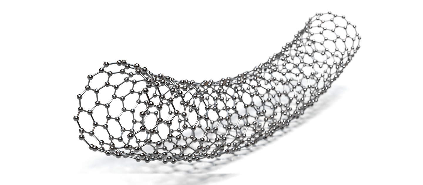
Introduced by IBM in 1998, carbon nanotubes (CNTs) are a relatively new electronic material compared to incumbent silicon. After almost a quarter-century of fundamental research and development, CNTs are now on the verge of breaking through into widespread use, and are already employed in large-scale circuits consisting of 10,000 devices. As Hersam and his teammates write, CNTs have several standout advantages, including chemical stability, scalability down to molecular-scale dimensions, and superb electrical and thermal properties.
However, there are remaining obstacles for materials scientists to overcome, the researchers wrote, to maximize CNTs’ potential. One challenge is purifying the CNTs, which can be either metallic or semiconductors. Additionally, the CNTs’ chiral vector imposes well-defined quantum-mechanical boundary conditions on the electronic band structure that implies, for random tube closure, around 33 percent of CNTs’ chiralities are metallic and around 67 percent are semiconducting. Because transistors require semiconducting channels, preferably with a well-defined and uniform band gap, the ability to scalably synthesize and isolate them with atomically precise chiral vector control is critical to realizing high-performance carbon nanotube transistor ICs.
Between the opportunities in high-performance digital logic with the potential for 3D integration and the possibilities for printed and even recyclable thin-film electronics, CNT transistors warrant a renewed and even redoubled effort from academic, government, and industry contributors. These molecular transistor technologies are within reach, but only if the remaining challenges are surmounted by the scientific and engineering communities.
One factor aiding the CNTs’ adoption, according to the authors, is expected advances in materials technology. For one, the CNTs’ purity must be improved, overcoming the lack of high-throughput analytical methods for detecting ultralow concentrations of metallic CNTs. There must also be advances in finding a scalable manufacturing approach to produce enough ultrahigh purity semiconducting CNTs to meet the potentially large market represented not only by high-performance IC but also high-volume printed electronics.
“Ultimately, growth conditions encompass such a vast parameter space that methods for efficiently searching and identifying optimal growth conditions are needed,” the authors wrote. “Emerging artificial intelligence and machine learning (ML) optimization approaches coupled with high-throughput experimental screening hold promise for next-generation synthetic efforts. Similarly, the discovery, optimization, and integration of the many other materials in a CNT transistor (including dopants, contacts, gate electrodes, and dielectrics) can also likely be accelerated by ML coupled with high-throughput experimental screening.”
Those efforts, Hersam and his collaborators wrote, is worth the time.
“Between the opportunities in high-performance digital logic with the potential for 3D integration and the possibilities for printed and even recyclable thin-film electronics, CNT transistors warrant a renewed and even redoubled effort from academic, government, and industry contributors,” the authors wrote. “These molecular transistor technologies are within reach, but only if the remaining challenges are surmounted by the scientific and engineering communities.”