Scientists Create Atomically Thin Metallic Boron
Synthesis of borophene expands family of two-dimensional materials beyond graphene
A team of scientists from the U.S. Department of Energy’s (DOE) Argonne National Laboratory, Northwestern University and Stony Brook University has, for the first time, created a two-dimensional sheet of boron -- a material known as borophene.
Scientists have been interested in two-dimensional materials for their unique characteristics, particularly involving their electronic properties. Borophene is an unusual material because it shows many metallic properties at the nanoscale even though three-dimensional, or bulk, boron is nonmetallic and semiconducting.
Because borophene is both metallic and atomically thin, it holds promise for possible applications ranging from electronics to photovoltaics, said Argonne nanoscientist Nathan Guisinger, who led the experiment. “No bulk form of elemental boron has this metal-like behavior,” he said.
The study will be published Dec. 18 by the journal Science.
 Like its periodic table neighbor carbon, which appears in nature in forms ranging from humble graphite to precious diamond, boron wears a number of different faces, called allotropes. But that’s where the similarities end. While graphite is composed of stacks of two-dimensional sheets that can be peeled off one at a time, there is no such analogous process for making two-dimensional boron.
“Borophenes are extremely intriguing because they are quite different from previously studied two-dimensional materials,” Guisinger said. “And because they don’t appear in nature, the challenge involved designing an experiment to produce them synthetically in our lab.”
Although at least 16 bulk allotropes of boron are known, scientists had never before been able to make a whole sheet, or monolayer, of borophene. “It’s only in the recent past that researchers have been able to make tiny bits of boron at the nanoscale,” said Andrew Mannix, a Northwestern graduate student and first author of the study. “This is a brand new material with exciting properties that we are just beginning to investigate.”
“Boron has a rich and storied history and a very complicated chemistry,” added Mark Hersam, professor of materials science and engineering at Northwestern’s McCormick School of Engineering and Applied Science, who helped advise Mannix. “This is something that could have easily not worked, but Andy had the courage and persistence to make it happen.”
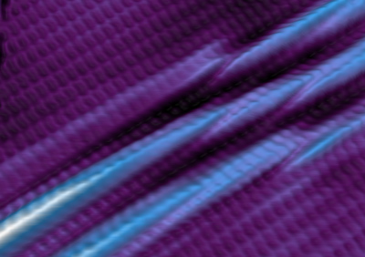
One of boron’s most unusual features consists of its atomic configuration at the nanoscale. While other two-dimensional materials look more or less like perfectly smooth and even planes at the nanoscale, borophene looks like corrugated cardboard, buckling up and down depending on how the boron atoms bind to one another, according to Mannix.
The “ridges” of this cardboard-like structure result in a material phenomenon known as anisotropy, in which a material’s mechanical or electronic properties -- like its electrical conductivity -- become directionally dependent. “This extreme anisotropy is rare in two-dimensional materials and has not been seen before in a two-dimensional metal,” Mannix said.
 Based on theoretical predictions of borophene’s characteristics, the researchers also noticed that it likely has a higher tensile strength than any other known material. Tensile strength refers to the ability of a material to resist breaking when it is pulled apart. “Other two-dimensional materials have been known to have high tensile strength, but this could be the strongest material we’ve found yet,” Guisinger said.
The discovery and synthesis of borophene was aided by computer simulation work led by Stony Brook researchers Xiang-Feng Zhou and Artem Oganov, who is currently affiliated with the Moscow Institute of Physics and Technology and the Skolkovo Institute of Science and Technology. Oganov and Zhou used advanced simulation methods that showed the formation of the crinkles of the corrugated surface.
“Sometimes experimentalists find a material and they ask us to solve the structure, and sometimes we do predictions first and the experiment validates what we find,” Oganov said. “The two go hand-in-hand, and in this international collaboration we had a bit of both.”
“The connection we have between the institutions allows us to achieve things that we couldn’t do alone,” Hersam added. “We needed to combine scanning tunneling microscopy with X-ray photoelectron spectroscopy and transmission electron microscopy to both obtain a view of the surface of the material and verify its atomic-scale thickness and chemical properties.”
As they grew the borophene monolayer, the researchers discovered another advantage within their experimental technique. Unlike previous experiments that used highly toxic gases in the production of nanoscale boron-based materials, this experiment involved a non-toxic technique called electron-beam evaporation, which essentially vaporizes a source material and then condenses a thin film on a substrate -- in this case, boron on silver.
“When we did our theoretical work, I had doubts as to the feasibility of obtaining two-dimensional boron because boron likes to form clusters, and ironing it out into two-dimensions I thought would be challenging,” Oganov said. “It turned out that growing on the substrate was key, because the boron and silver turn out not to react with each other.”
The experimental work was funded by the DOE’s Office of Science and was performed at Argonne’s Center for Nanoscale Materials, a DOE Office of Science user facility, and at the Northwestern University Materials Research Center.