MNDL Team Propose New Research Method in Nature Scientific Reports
The method, called “objective-first inverse design” could pave the way to the design of ultra-compact devices with ever more complex optical functionalities.
A Northwestern Engineering team recently found a way to have computers design nanophotonic devices without any human input.
Nanophotonic devices are few-microns scale devices that can achieve desired optical functionalities, converting a given input into a desired output, with many applications in optical communications, sensing, lighting, displays… For decades, researchers have designed nanophotonic devices based on intuition and trial-and-error.
 But now Prof. Koray Aydin has proposed to replace the researcher’s intuition by computing power for the design of nanophotonic devices. The method, called “objective-first inverse design” could pave the way to the design of ultra-compact devices with ever more complex optical functionalities.
“It would take the world’s computing power for universe’s lifetime to test all the devices that can be made in a design space of 100 pixels only, so imagine for 10,000 pixels or more!” said Aydin, Professor in the Electrical Engineering and Computer Science Department and director of the Metamaterials and Nanophotonic Devices Laboratory (MNDL). “We need a smart algorithm to explore the entire design space and quickly find the best design to achieve the desired functions, and our inverse-design method just does that.”
The team used their method to design an optical diode, a device that transmits light in one direction but reflects light coming from the other direction, which is very hard to design with other methods.
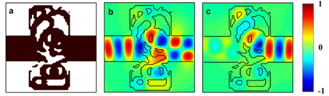
 “Our design is not intuitive at all because it comes out of the brain of a computer, but it shows three times enhanced bandwidth within a footprint which is five times lower than similar devices based on photonic crystals,” said Francois Callewaert, a PhD student in Aydin’s lab. “This shows the potential of the method to design complex functions within extremely small structures.”
Supported by Northwestern’s Materials Research Science and Engineering Center (MRSEC), the McCormick School of Engineering and Applied Sciences and the Institute for Sustainability and Energy at Northwestern (ISEN), their research, titled, "Inverse Design of an Ultra-compact Broadband Optical Diode Based on Asymmetric Spatial Mode Conversion" has been published in the September issue of Nature Scientific Reports. Callewaert is first author and Dr. Serkan Butun, a postdoctoral fellow and Zhongyang Li, PhD student in MNDL are co-authors.
“This is just the beginning of the story”, Aydin concludes. “Given the versatility of the method, we are only limited by our imagination, and we are working on the design of various other devices that will have very useful properties for on-chip communications and for the control of light at the nanoscale in general, so stay tuned.”