Researchers Develop World’s Highest Quantum Efficiency UV Photodetectors
Advance in ultraviolet detection technology could aid early missile detection, chemical and biological threat detection
Researchers from Northwestern University’s McCormick School of Engineering and Applied Science have developed the world’s highest quantum efficiency ultraviolet (UV) photodetector, an advance in technology that could aid in the detection of missiles and chemical and biological threats.
The development of UV photodetectors has been driven by numerous applications in the defense, commercial, and scientific arenas. Until recently, photomultiplier tubes or silicon photodectors with UV band-pass filters were the only viable options for imaging in this important spectral range. Thanks to technological and scientific advances in the III-Nitride material system, high aluminum composition AlxGa1-xN-based semiconductor structures have become a promising alternative.
 Manijeh Razeghi, Walter P. Murphy Professor of Electrical Engineering and Computer Science at McCormick, and her group have brought this AlxGa1-xN-based dream device closer to reality by developing a compact photodetector with the world’s highest quantum efficiency.
“Heat sources such as flames, jet engines, or missile plumes emit light throughout the UV portion of the spectrum corresponding to their black-body temperature,” said Razeghi, director of Northwestern’s Center for Quantum Devices. “These manmade UV sources can easily be detected at wavelengths less than 290 nanometers due to the non-existence of a terrestrial background signature. The military, in particular, is interested in developing ground- and air-based solar-blind sensors to detect the UV signature of an active missile plume and provide early warning and potentially allow for missile tracking and ultimately interception.”
The military could also use the UV detectors and sources to detect biological threats.
“Biological agents could have devastating effects on public health, as the anthrax scare of 2001 made us all too aware,” said Erdem Cicek, a graduate student in Razeghi’s lab. “There is a significant lag time between a covert attack and the widespread appearance of symptoms, which makes the general lack of readily available real-time detection systems a significant problem. The low-cost UV photodetectors we developed can be used as a critical weapon in the defense against a bio-terror attack, allowing authorities time to warn the population, identify the contaminated areas, and enact quarantine procedures before the exposure overwhelms response capabilities.”
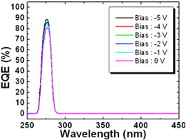
Conventionally, AlxGa1-xN-based solar-blind photodetector structures are grown at a reactor pressure of 50 millibar. Razeghi’s group observed that reducing the growth pressure helps to suppress parasitic pre-reactions and yields more manageable growth rates while still maintaining good material quality. By refining the low-pressure metal-organic chemical-vapor-deposition growth as well as the UV photodetector p-i-n structure, Razeghi’s group has successfully fabricated the world’s highest quantum efficiency solar-blind UV photodetectors grown on sapphire substrate (Fig. 1).
A paper describing the results, “AlxGa1-xN-Based Back-Illuminated Solar-Blind Photodetectors with External Quantum Efficiency of 89%,” was published November 5 in the journal Applied Physics Letters.
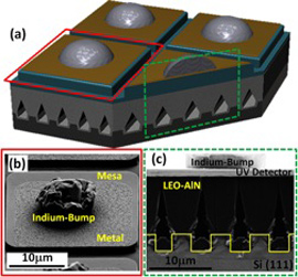
Although sapphire is the most common choice for back-illuminated devices, researchers also developed alternative low-cost UV photodetectors grown on silicon substrate. Razeghi’s group used a novel maskless Lateral Epitaxial Overgrowth (LEO) technique for the growth of a high-quality aluminum nitride (AlN) template layer on silicon substrate. Following the template growth, a p-i-n structure is grown and processed. The flip-chip hybridized and substrate-removed array is shown in Fig. 2.
This low-cost approach eventually led to the world’s first successful implementation of UV-PD structure grown on a silicon substrate. A paper describing the findings, “AlxGa1-xN-Based Solar-Blind Photodetector Based on Lateral Epitaxial Overgrowth of AlN on Si Substrate,” was published October 30 in the journal Applied Physics Letters.
The researchers will now work to achieve higher than 95 percent operability UV focal plane array with high uniformity.
The research is supported by the US Navy.